The Sheet of Glass That Determines the Price
The mother-glass generation a fab chooses before pouring concrete determines which panel sizes are profitable — and which competitors can undercut you — for the next decade.
The Arithmetic of the Mother Glass
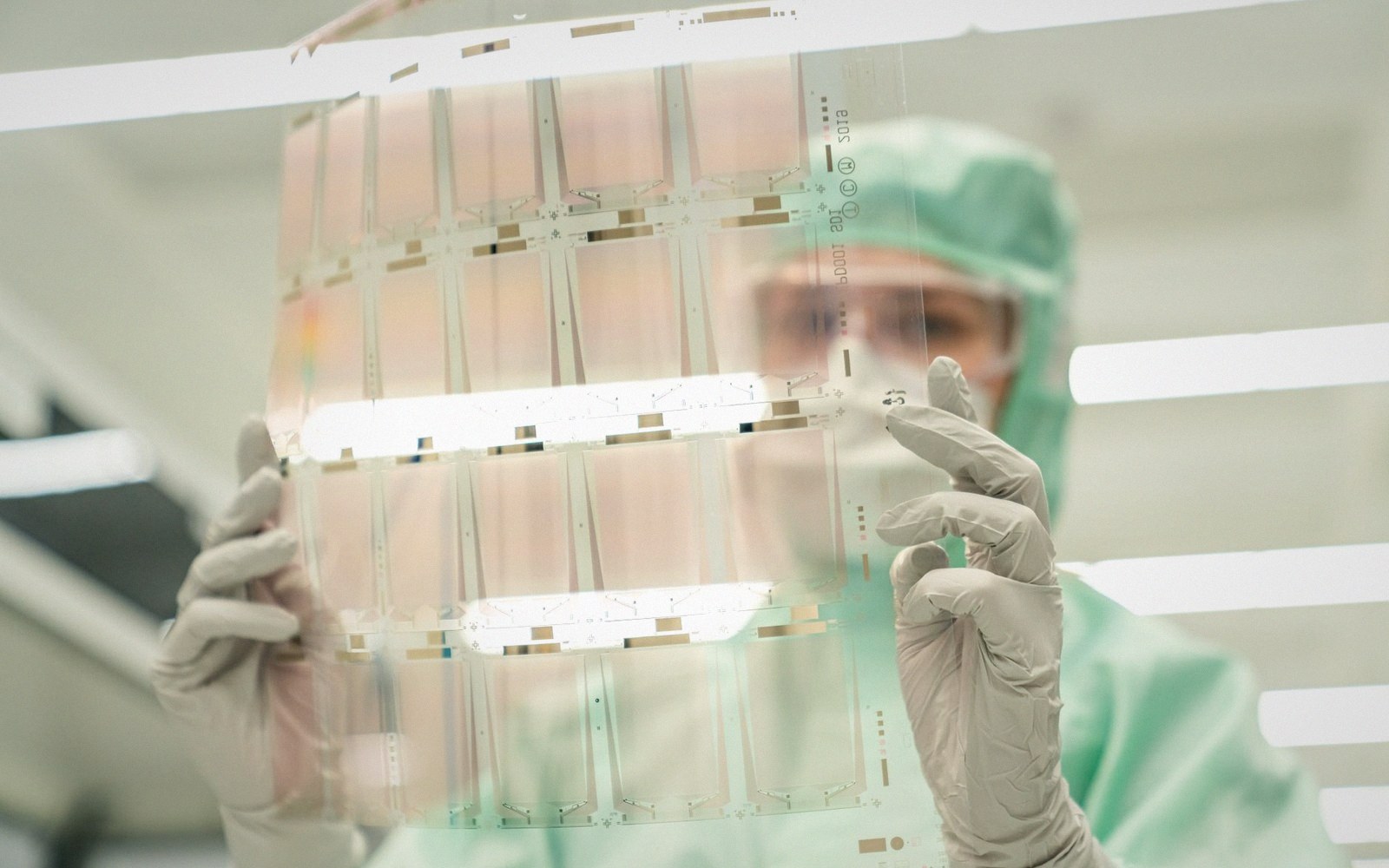
Every LCD panel starts life as a rectangular sheet of ultra-thin aluminosilicate glass, deposited with TFT arrays, colour filters, and alignment layers before being cut into individual display panels. The industry numbers these sheets by generation, where each generation simply specifies a standard substrate dimension. Gen 6 runs roughly 1,500 × 1,850 mm. Gen 8.5, the workhorse of the flat-panel era, sits at 2,200 × 2,500 mm. Gen 10.5 — the format BOE, CSOT, and Sharp-Foxconn have committed billions to — measures 2,940 × 3,370 mm, a sheet large enough to park a small car on.
The number that actually matters is utilisation: the fraction of the mother glass converted into saleable panel area, with as little scrap as possible. A panel size that tiles neatly onto a substrate — in display engineering, "good fit" — means high utilisation and low unit cost. A panel size that leaves awkward offcuts is wasteful enough to shift the entire cost structure of a product line.
The arithmetic is straightforward. A Gen 8.5 substrate cuts six 55-inch panels with utilisation above 95 %. Cut 65-inch panels from the same glass and you get only three, so the fit degrades and scrap climbs. Switch to a Gen 10.5 fab and 65-inch becomes an eight-up cut at high utilisation; 75-inch yields six. The jump in substrate area — Gen 10.5 carries roughly 80 % more glass than Gen 8.5 — does not merely permit larger panels; it fundamentally reprices them. A 65-inch panel built on Gen 10.5 glass costs materially less to produce than the same size cut from Gen 8.5, because more panels share the fixed cost of one process cycle.
Why Fabs Lock In Economics for a Decade
Building a Gen 10.5 fab requires capital expenditure in the range of $7–9 billion USD per facility, with a construction and ramp timeline measured in years. The tools — sputtering systems, PECVD chambers, exposure machines for photolithography — are specified to a fixed substrate format. You cannot change the glass size after the fact without rebuilding around it. Every process recipe, every robot arm, every cassette carrier, and every inspection system is dimensioned to the chosen generation.
This means a manufacturer's substrate-generation decision is effectively a bet on which panel sizes the market will want across the facility's operating life, typically fifteen to twenty years. Get the bet right — as Samsung did with Gen 8.5 during the 32-to-55-inch TV expansion of the 2000s and 2010s — and the utilisation advantage funds years of margin. Get it wrong, or stay loyal to an older generation too long, and competitors with better-fitting glass systematically undercut your cost per square metre.
The Chinese panel makers understood this precisely when they committed to Gen 10.5 around 2016–2018. At the time, 65-inch and 75-inch TV penetration was rising fast. A Gen 8.5 incumbent cutting 65-inch panels at suboptimal utilisation would face a structural cost disadvantage against any Gen 10.5 entrant cutting the same size at peak utilisation — regardless of other operational efficiencies. The substrate generation created the price floor; everything else was secondary.
Glass Quality Is Not a Free Variable
Larger substrates demand glass with tighter dimensional tolerances. Thermal expansion during processing must be predictable across nearly three metres of glass — a coefficient of thermal expansion (CTE) mismatch between the glass and the deposited TFT layers introduces stress that causes defects. Corning's Eagle XG and NEG's G10 product families target CTEs around 3.8 × 10⁻⁶ per °C, precisely matched to the silicon nitride and indium gallium zinc oxide (IGZO) layers deposited on top. Any bow or warp in the substrate at Gen 10.5 scale compounds into alignment errors that the TFT backplane exposure tools must compensate for across the full sheet.
Glass thickness has also fallen over generations — modern substrates run 0.5 mm or thinner — because thinner glass flexes less under its own weight when handled horizontally and reduces module thickness. The tradeoff is handling fragility; Gen 10.5 sheets at 0.5 mm are genuinely difficult to transport and load without robotic handling throughout, which adds to the fab's capital requirements and raises the minimum viable production volume needed to service the debt.
Yield integrates across every layer process and every square millimetre of substrate. A particle contamination event that kills one panel on a six-up Gen 8.5 cut costs one-sixth of the substrate. The same event on an eight-up Gen 10.5 cut costs one-eighth — but the absolute cost of the substrate is larger, so the economic pressure to maintain clean-room yield is, if anything, higher.
The substrate generation is, in the end, a manufacturing commitment disguised as an engineering choice. It sets the cost floor for every panel that emerges from the fab, defines which competitors the operator can match on price, and constrains the product mix for as long as the building stands. The glass decides.